Silicon Wafer Reclaim
Kyushu Dentu (KDK) has entered the silicon wafer reclaim business by leveraging its long-standing expertise in crystal polishing and processing.
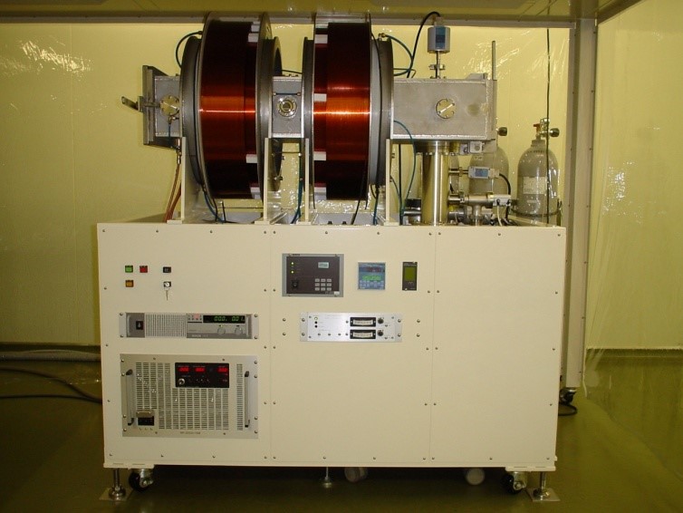
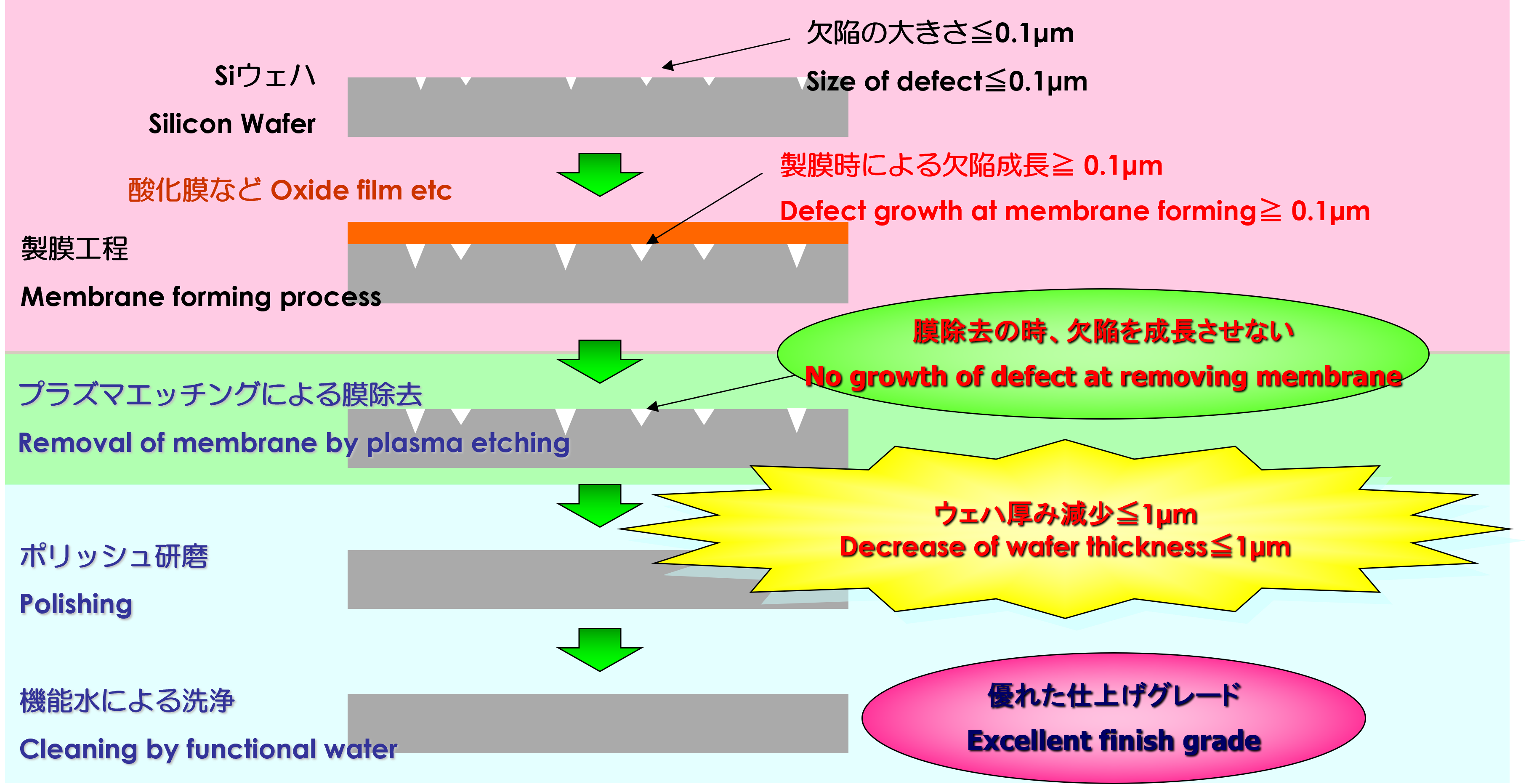
By enhancing our proprietary plasma equipment, originally developed for high-frequency crystal processing, we have established a technology for removing films from 12-inch silicon wafers. Unlike conventional wafer reclaim processes that rely on chemical treatments, our method does not use such chemicals, resulting in lower damage and a more environmentally friendly process. This enables a significant improvement in the number of reclaim cycles.
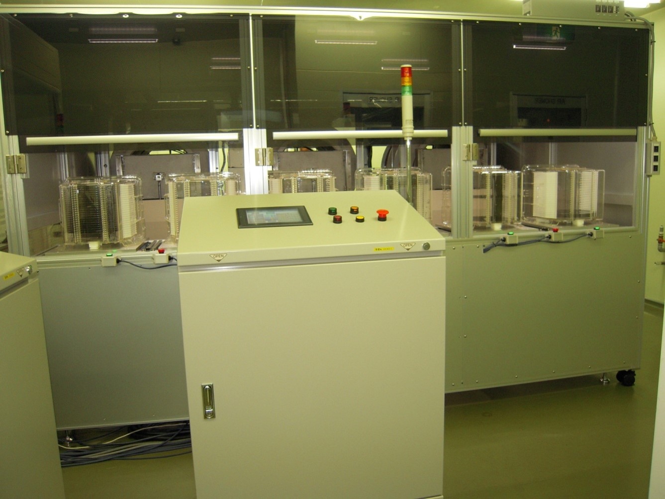
In addition to silicon wafer reclaim services, we also offer the development and sales of plasma etching equipment. Please feel free to contact us for more information.
Technology of Plasma Etching
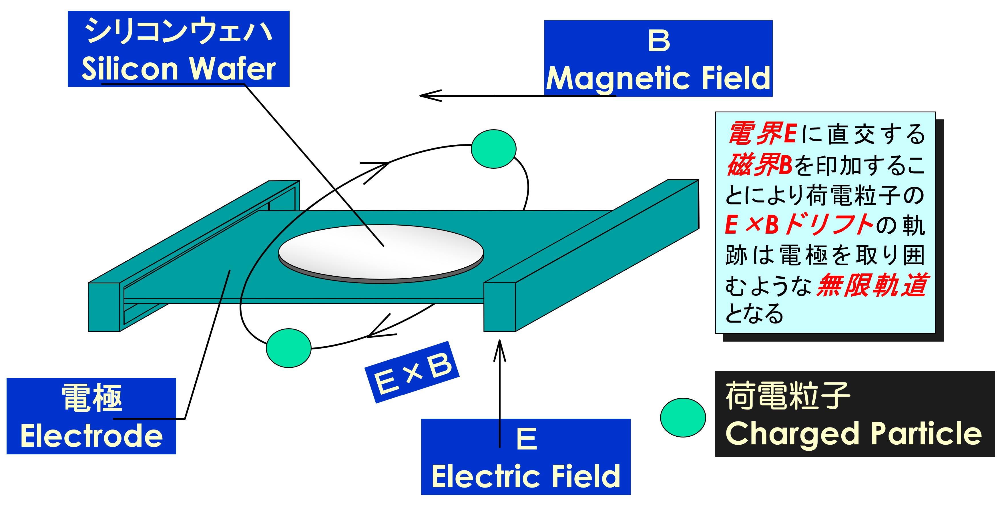
Kyushu Dentsu (KDK)’s silicon wafer reclamation technology utilizes a proprietary low-damage plasma dry process to accurately restore wafer surfaces, contributing to increased reuse cycles and reduced costs.
Plasma Etching Feature Summary
| Features | Benefits |
|---|---|
| No use of special chemicals (e.g., HF) | No waste liquid treatment required, reducing environmental impact |
| Uniform plasma processing | Excellent surface restoration performance |
| Minimal wafer thickness reduction (approx. 1 μm) | Significantly improves reclaim efficiency and reduces running costs |
| Low material removal during processing | Efficient use of resources and contributes to environmental sustainability |
Plasma Etching Feature1
Plasma Etching Feature2
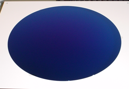
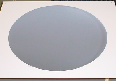
Plasma Etching Before After

Silicon Wafer Reclaim Video
Plasma Etching Machine